 Fraunhofer USA Center Midwest CMW
Chemical Sensing
General Chemical Sensing
Electrochemical sensors are powerful and versatile tools that can detect a wide range of analytes in a variety of applications. At CMW, our work revolves around two main areas of focus:
Biochemical Measurements
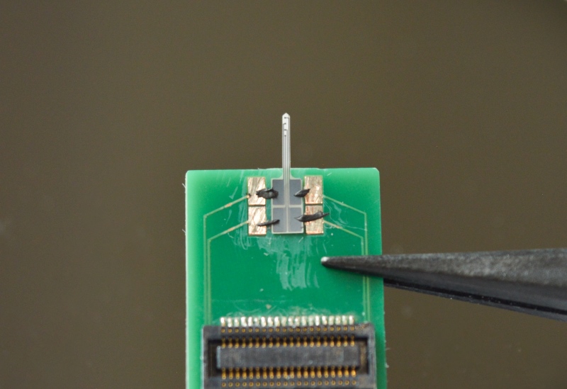
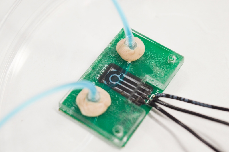
Prototype all diamond microelectrode array on a custom-made PCB
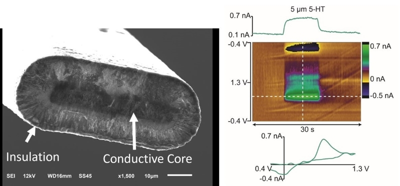
Left, all diamond microelectrode with a conductive BDD core, and intrinsic polycrystalline insulation layer. Right, representative FSCV response on the BDD microelectrode for serotonin.
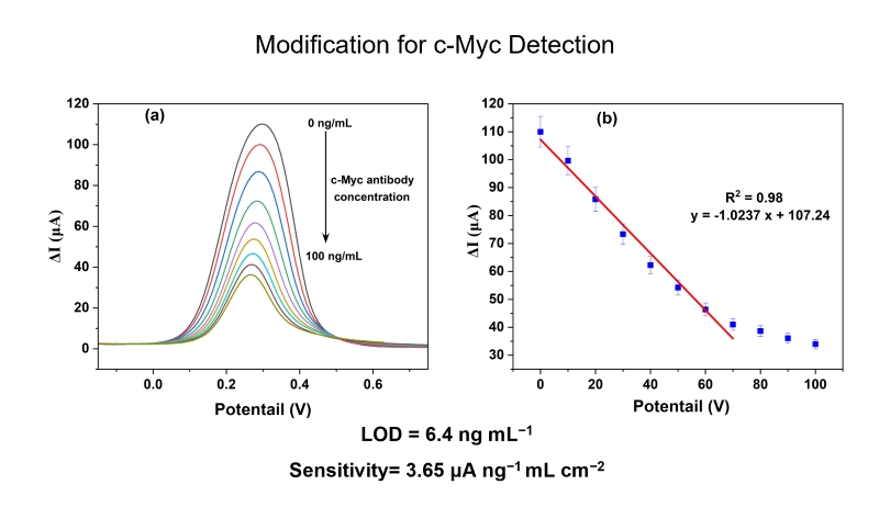
Differential pulse voltammetry response showcasing the linear binding of an antibody onto a BDD surface
We specialize in the detection of bio electroactive metabolites like dopamine and serotonin using fast-scan cyclic voltammetry (FSCV), which allows for high-resolution, real-time monitoring. For non-electroactive metabolites and biomarkers, we use surface modifications and biomolecule attachment to develop both label-free and sandwich-type electrochemical immunoassays. By immobilizing bio-recognition elements or using electroactive tags, we enable selective, sensitive detection across diverse sample types.
Environmental Measurements
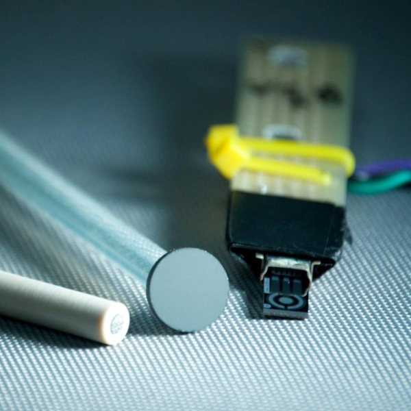
BDD based 3in1 electrode on a Si substrate
Packaged BDD 3in1 in a microfluidic system for flow through measurements
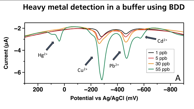
Heavy metal response for Hg 2+, Cu 2+, Pb 2+, and Cd2+ on a BDD electrode
Our sensors detect various electrochemically active species, including heavy metals like Pb²⁺, Cd²⁺, Cu²⁺, and Hg²⁺. In addition, we use surface modification techniques to create pH sensors. Furthermore, we use electrochemical advanced oxidation processes (EAOPs) to release and detect bound contaminants, providing a deeper understanding of environmental systems.
Diamond Sensors
Prototype demonstrators of BDD electrodes. Left: BDD in PEEK, Center: BDD disk electrode, Right: BDD 3in1 with a custom electrical adapter.
Boron-doped diamond (BDD) is a unique and robust electrode material with a large potential window in aqueous solution and low background current. With its resistance to electrochemical fouling and wider potential window with a lower background current, BDD material is an attractive surface for electrochemical analysis experiments. It is a green and renewable surface through acid cleaning and activation for repeated experiments.
We developed a large portfolio of boron-doped diamond electrodes and materials targeting a broad range of markets, including biotechnology, environmental, and health. The available portfolio is offered to collaborators and project partners to further advance the technology and develop products. These electrodes are made by growing in-house CVD polycrystalline diamond, and through wafer processing techniques such as lithography and reactive ion etching, we can structure these into a variety of 2D shapes and sizes to meet your needs.
With a lower capacitive background current and wider potential window to other competing electrode materials, such as glassy carbon (GC), our BDD electrodes can be used for electroanalytical measurements with ease. BDD has advantages over a variety of electrode materials, including GC because of the flat background, enabling a broader range of measurements.
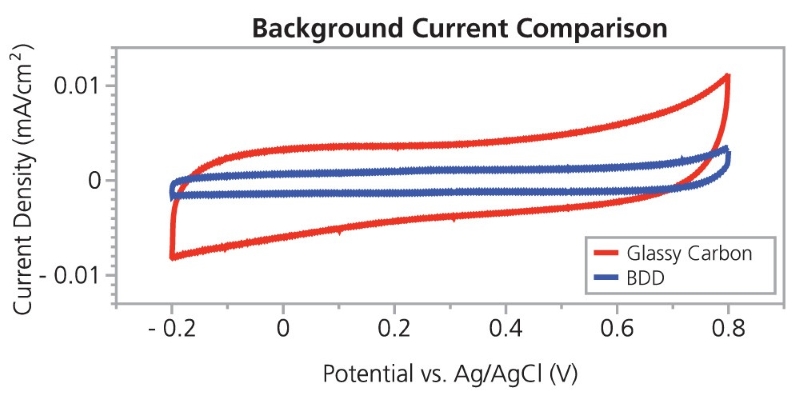
BDD electrochemical background comparison towards glassy carbon in 1M KCl
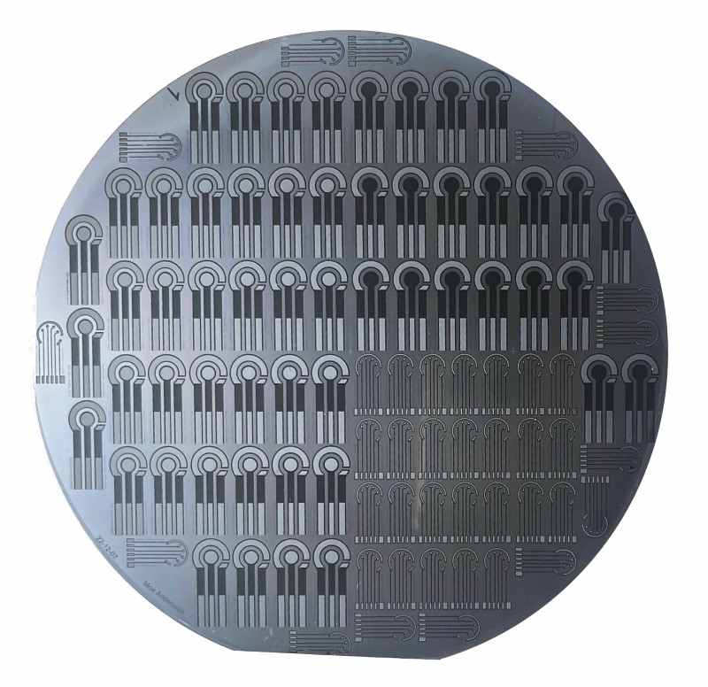
BDD 4in silicon wafer microfabricated into a variety of geometries and dimensions of electrochemical sensors.
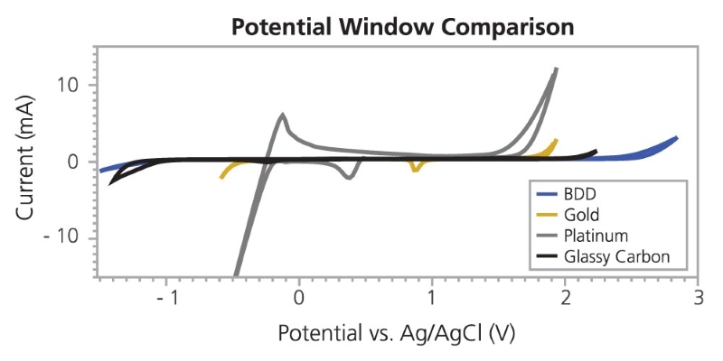
Comparison of several working electrode materials in 1 M H2SO4 showcasing BDD’s advantages
Disk Electrodes
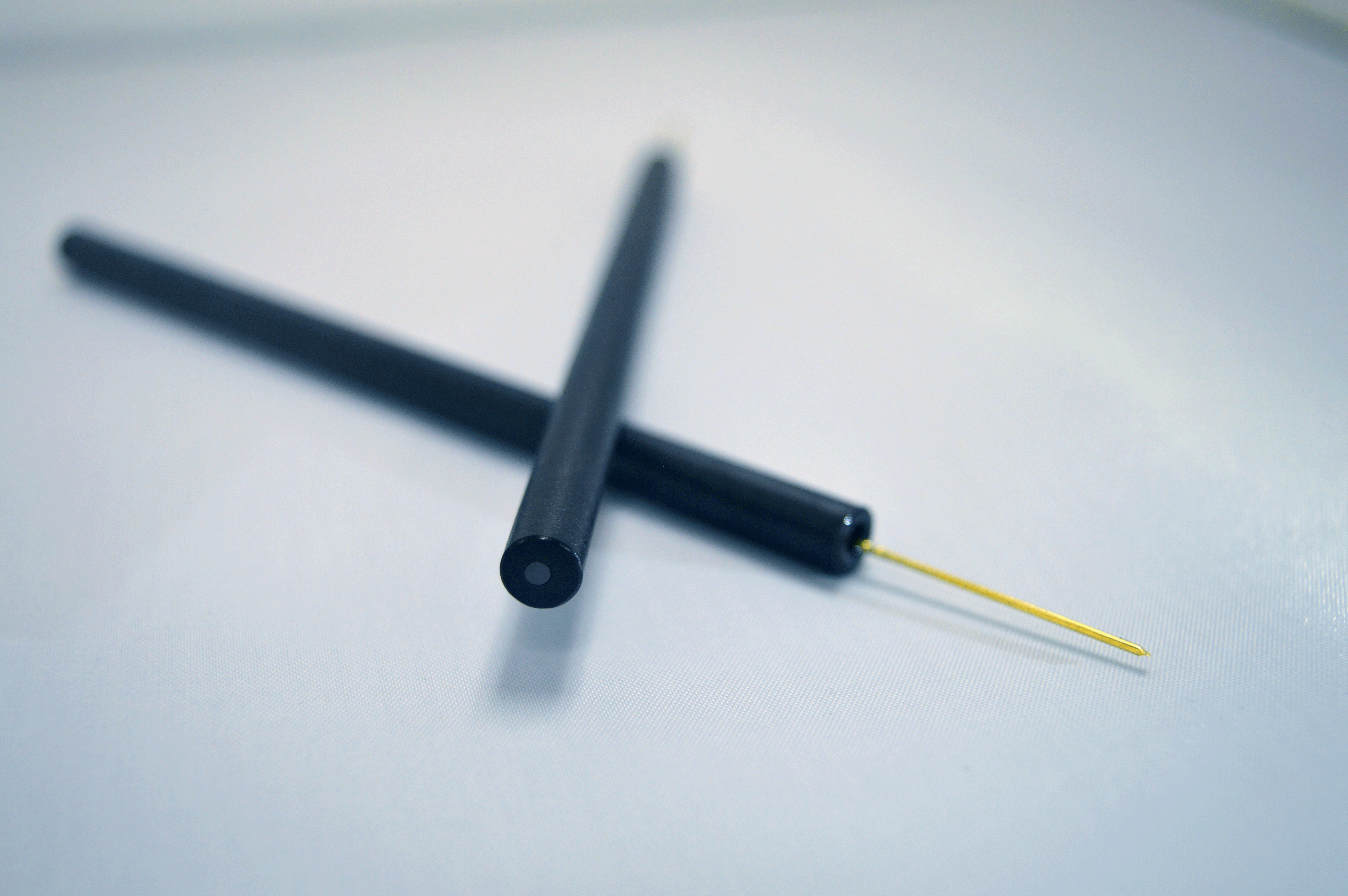 2mm BDD electrode packaged into a PEEK housing
BDD disk electrodes offer superior electrochemical performance to other commercially available electrodes. Standard electrodes embed a 2mm polished BDD disk in a 6cm long x 6mm outer diameter PEEK housing. Custom orders with other chemical resistant housings, including PTFE, are possible.
Diamond Plates
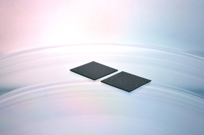 10 x 10 mm BDD freestanding plate electrodes
Both BDD grown to varying thicknesses on either conductive or insulating silicon as well as free-standing BDD plates are available for a variety of applications. These plates can be modified to fit specific experimental needs. BDD plates exhibit high electrical conductivity that is maintained at elevated temperatures, excellent mechanical and chemical rigidity, and long-lifetime. BDD on silicon can be grown as thick as 40 µm. Freestanding BDD plates are grown to 350 μm thick. Both materials are as-grown and unpolished. The material is typically offered in 10 mm x 10 mm geometries, but smaller and larger geometries can be accommodated through laser dicing.
Boron-Doped Diamond Optically Transparent Electrodes
 BDD OTE film on a quartz substrate
Combining the advantage of rugged BDD material with optical transparency, BDD optically transparent electrodes (OTEs) are excellent tools for spectroelectrochemical measurements. Applications range from the general study of redox chemistry (inorganic, organic, biological molecules) to spectroelectrochemical sensing where excellent sensitivity and selectivity can be obtained.
The BDD films are grown on quartz substrates and exhibit a wide range of optical transparency. Measurements can be made below 300 nm, a quality certain OTE materials can not achieve. The optical and electronic properties can be altered depending on experimental requirements; a more conductive film will be less optically transparent, while a more optically transparent film will be less conductive. Custom dimensions including microfabrication can be accommodated to fit a specific geometry.
Custom Electrode Fabrication Capabilities
Boron-doped diamond (BDD) fabrication capabilities range from diamond growth via post-growth fabrication to assembly and material evaluation. BDD films can be applied to a variety of substrate materials and geometries ranging from small (micron ) to large (4” Si wafer) substrates. Post diamond growth capabilities include polishing, photolithography, etching, metallization, and laser-cutting.
Diamond is grown on a variety of substrates, including but not limited to certain metals (including expanded metal mesh), quartz, pyrex, silicon, and polycrystalline diamond. With the application and product in mind, substrates are carefully evaluated and individually pre-treated for optimized diamond growth and resulting diamond materials. In-house clean room microfabrication processes allow for 4” diameter wafer processing including PVD (metallization) and PE-CVD (SiO2 ) thin film deposition, photolithography and plasma etching.
Diamond lapping, polishing and laser cutting complement the Center's capabilities, striving towards a one-stop solutions provider for BDD electrode development and prototypes.
Custom Instrumentation and Setup
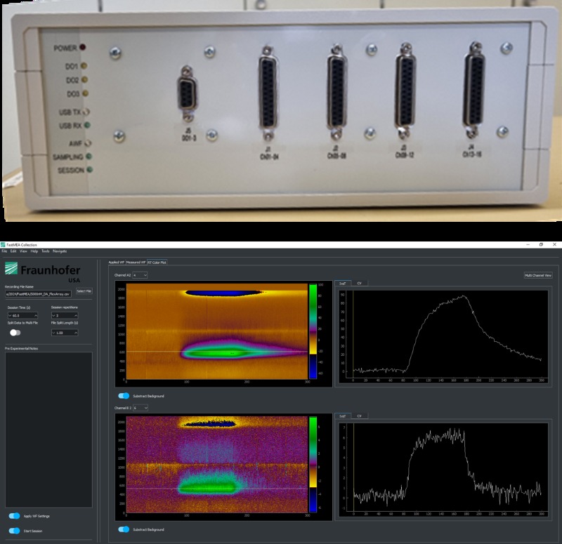
FastMea FSCV recording system with GUI
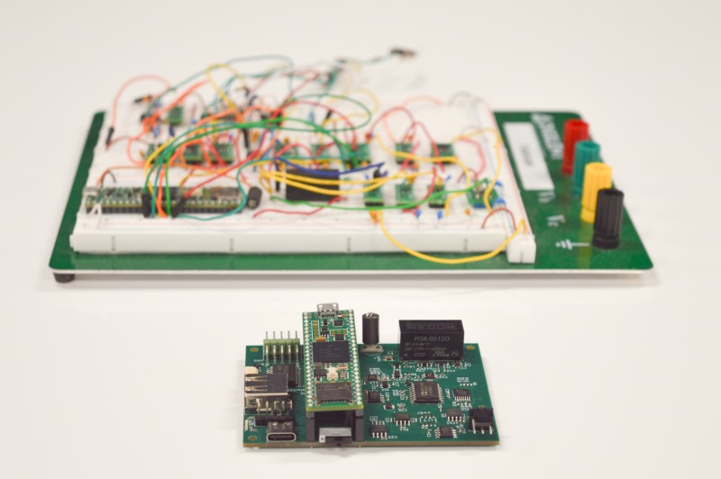
From concept to a PCB prototype chemical instrument
Often electrodes and instrumentation need to be fabricated custom for the experimental setup and needs. The in-house fabrication equipment provides great flexibility and enables us to design tailor the measurement needs. Through custom microcontroller programing, to electronics design, CMW has built microcontroller based potentiostats utilizing python interface software. CMW also specializes in providing wholistic solutions, such as designing electrode interfaces with microfluidics and instrumentation.
- Design of a microcontroller potentiostat, and iterating from bread board to printed circuit board for real-time heavy metal measurements.
- In collaboration with Fraunhofer Institute for Microelectronic Circuits and Systems, and Fraunhofer USA Center Mid-Atlantic, we developed a 16-channel Fast-scan cyclic voltammetry recording system for high-speed electrochemistry to measure dopamine on our diamond microelectrode arrays.