 Fraunhofer USA Center Midwest CMW
Diamond Materials
Epilayers
CMW has the expertise and technology to produce epilayers to target thickness and with p-type and n-type precision on (100) and (111) oriented SCD. Epilayer thickness offerings range from a few hundred nanometers to greater than 25 µm. CMW offers p-type doping with boron for doping concentrations ranging from trace level doping (~1E15 [B]/cm3) all the way to E21 [B]/cm3 for use as semi-metallic contact layer or to enable superconductivity. Supplemental offerings include low-material removal CMP of these epilayers to achieve near atomic flatness.
CMW also has the capability to perform selective growth of epilayers using SiO2 masks.
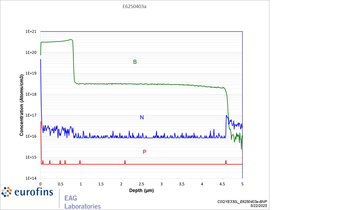
SIMS plot of a epilayer stack of a semiconductor level boron doped diamond epilayer covered by a heavily doped contact layer on an intrinsic diamond wafer.
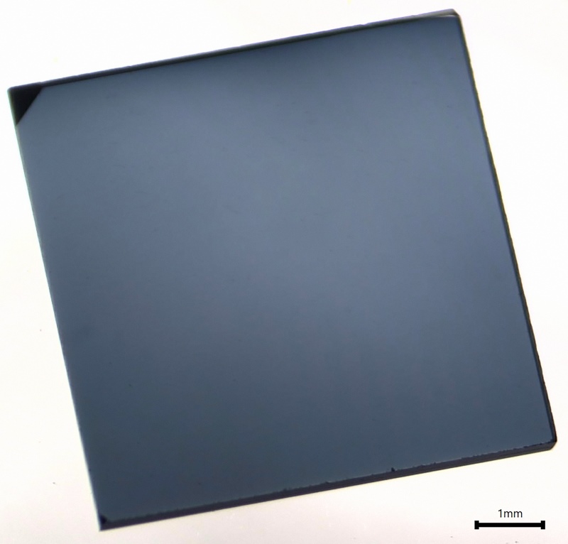
Image of a thin (approx. 2μm) heavily boron doped epilayer on intrinsic SCD wafer
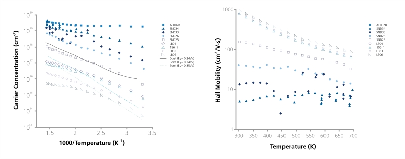
Temperature dependent carrier concentration and Hall mobility data of boron-doped diamond epilayers with varying boron doping concentrations.
Wafers and Crystals
CMW offers growth and fabrication of intrinsic and boron-doped SCD wafers for use in a variety of applications. Wafers can be further processed via CMP to achieve near atomic flatness and eliminate wafer bow.
CMW has developed a unique synthesis process that allows for growth of 300 – 500 µm thick freestanding boron-doped SCD wafers. These wafers are grown in one single growth step. This results in the minimization of killer defects, which would be detrimental for use in vertical devices.
Working with commercial partners, Fraunhofer USA, CMW can offer monosectorial intrinsic SCD wafers up to 1-inch square, and boron doped SCD wafers up to 8 mm x 8 mm. Current epilayer deposition expertise up to 12 mm node exists with ongoing expansion to 1-inch node.
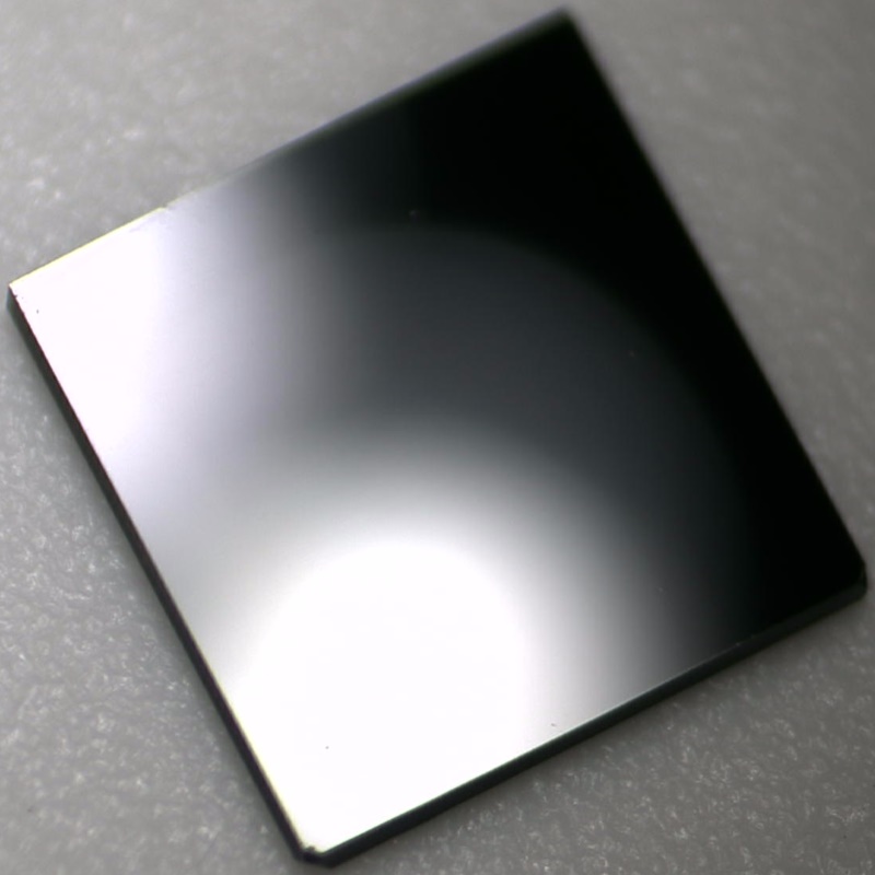
Image of a freestanding heavily boron doped SCD wafer with low electric resistance (mΩcm range)
Diamond Nanoparticles
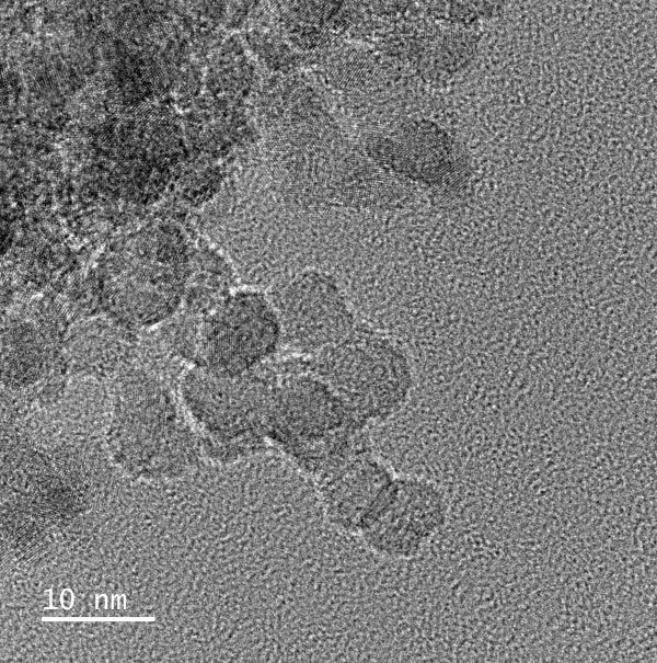
CMW has achieved size-controlled diamond nanoparticles (seen in the TEM image), with great promise for technologies such as biomedical imaging, advanced therapeutics, and quantum applications.
Diamond nanoparticle-based abrasives have been deployed industrially in a powder form or as pastes and suspensions. With the development of processes for the inclusion of color centers into these nanoparticles, their applications have expanded into biomedical applications, quantum sensing, and novel hybrid/composite materials. Examples include enhanced MRI contrast, multimodal in-vivo bioimaging, and the development of targeted cancer therapies. Broadly these particles can act as agents for both classical and quantum-based sensing, therapeutics for improvement of human health, and the development of exceptional composites. CMW focuses on diamond nanoparticles striving to improve processes essential to production of property-controlled diamond nanoparticles, and to integrate these particles into meaningful technologies.