 Fraunhofer USA Center Midwest CMW
One challenge that diamond continues to face is the unavailability of affordable, large area (inch-size) wafers that are suitable for applications that require high crystalline quality, such as optics, electronics and quantum. Fraunhofer USA Center Midwest (CMW), while continuously working on further lateral size expansion of SCD wafers, has developed diamond membranes that can be used to sidestep existing limitations with SCD wafers.
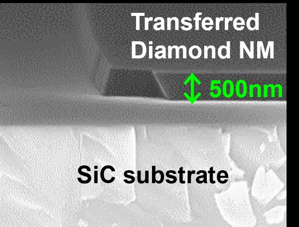
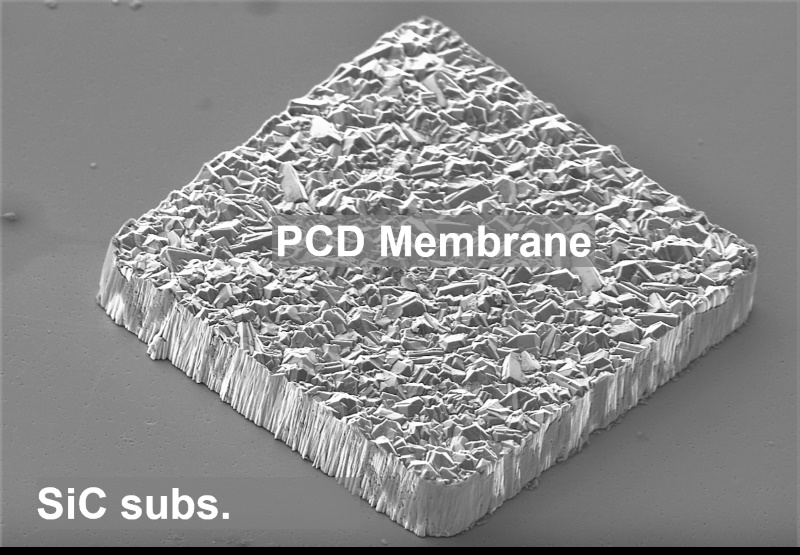
Semiconductor membranes are freestanding sheets of a semiconducting material that are only a few microns (µm) thick. These membranes possess the same properties as the corresponding bulk material (wafer), but the thinness of the membrane makes it flexible. This allows for seamless transfer and integration of these membranes with other semiconductor materials. Successful membrane transfer requires very smooth membrane and wafer surfaces, which can be achieved via the Fraunhofer USA CMW CMP process that was specifically developed for these types of technology. This time of assembling devices of different semiconductor materials is called heterointegration and allows for (i) upscaling of materials to wafer dimensions of mature materials, and (ii) being able to leverage intrinsic preferred properties of materials.
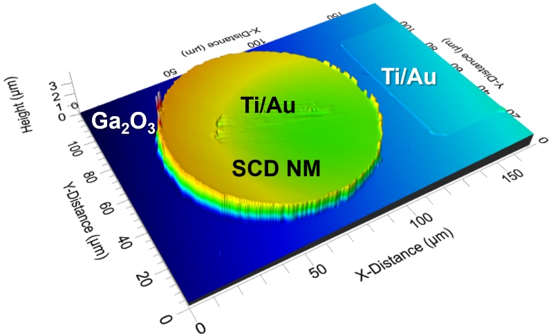
In case of diamond, it is possible to transfer active p-type diamond device areas onto pre-processed gallium nitride (GaN) and aluminum nitride (AlN) wafers. That way, the device will leverage diamond being a natural p-type material, while GaN and AlN are natural n-type materials. Further, it represents a size upscaling since all the diamond components can be synthesized and processed on a SCD wafer node that is currently available, and then upcycle to a multi-inch GaN or AlN wafer that is compatible with commercial microfabrication equipment.